
Future detectors for particle physics, astroparticle physics or photon science will have several billion electrical channels. Together with rapidly increasing data rates of the individual channels, this will lead to a massive increase in the data rate to many terabits per second. Processing these data volumes is one of the greatest challenges for future detector systems. Even with strong, local data reduction already in the detector, it will not be possible to transfer all raw data to the counting room using conventional technology. A key to mastering this challenge is an increased transmission bandwidth. This can be achieved with optical data transmission.
At the IPE we develop a universal system for a fast and energy-efficient transmission of very large amounts of data from detectors of large physics experiments. The key component is a photonic transmitter chip with electro-optical modulators which convert the electrical signals of the detector into optical output signals. These are transmitted via optical fibers to the receiver in the counting room. High transmission bandwidths per glass fiber are achieved by bundling optical channels using wavelength division multiplexing (WDM), as the data rate per channel is limited due to the required radiation hardness and low energy consumption.
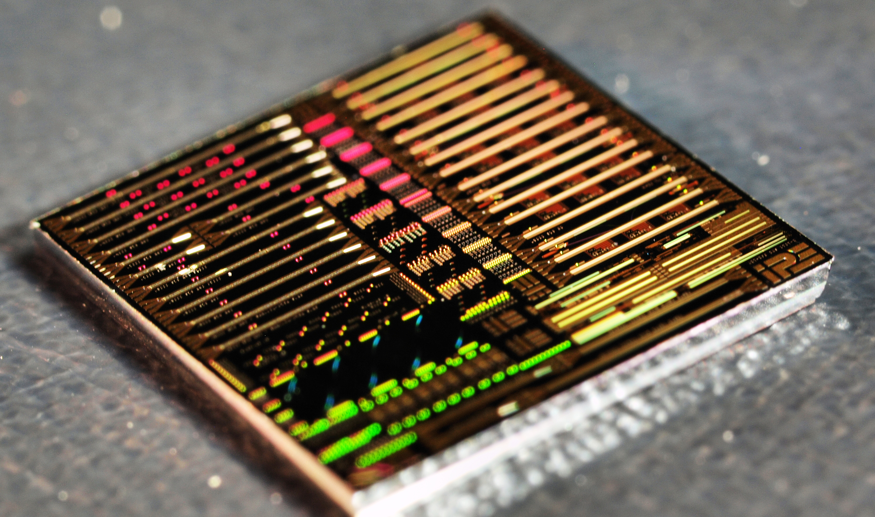
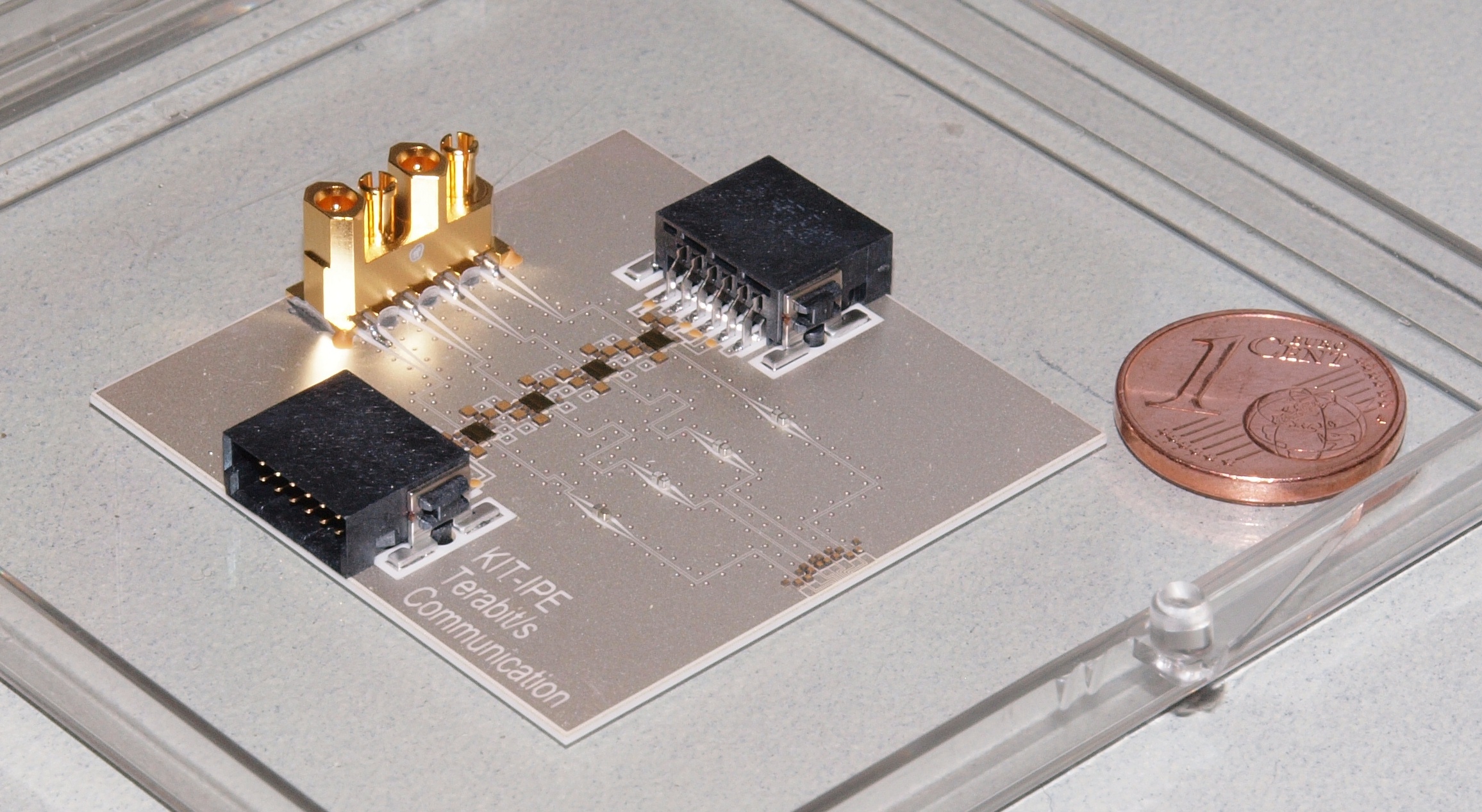
We develop the entire optical transmission system. On the one hand it consists of the transmitter chip with monolithically integrated electro-optical modulators, optical multiplexers and demultiplexers, thermal phase shifters, operating point control and optical couplers. The other two important elements are the electronic driver with included control electronics and parameterization and the optical receiver in the counting room. The use of transmitter chips in detectors also requires an adapted, reliable and very space-saving packaging technology withstanding low temperatures, strong magnetic fields and high radiation exposure. This is also being developed by us at the IPE.
Technology
In current systems, directly modulated laser diodes are used as transmitters. The modulated optical signal is transmitted via an optical fiber to a receiver in the counting room. The disadvantage of this technology is that each laser diode, i.e. each transmission channel requires an individual glass fiber. An additional challenge when used in particle detectors is that laser diodes under particle bombardment have a very limited life time.
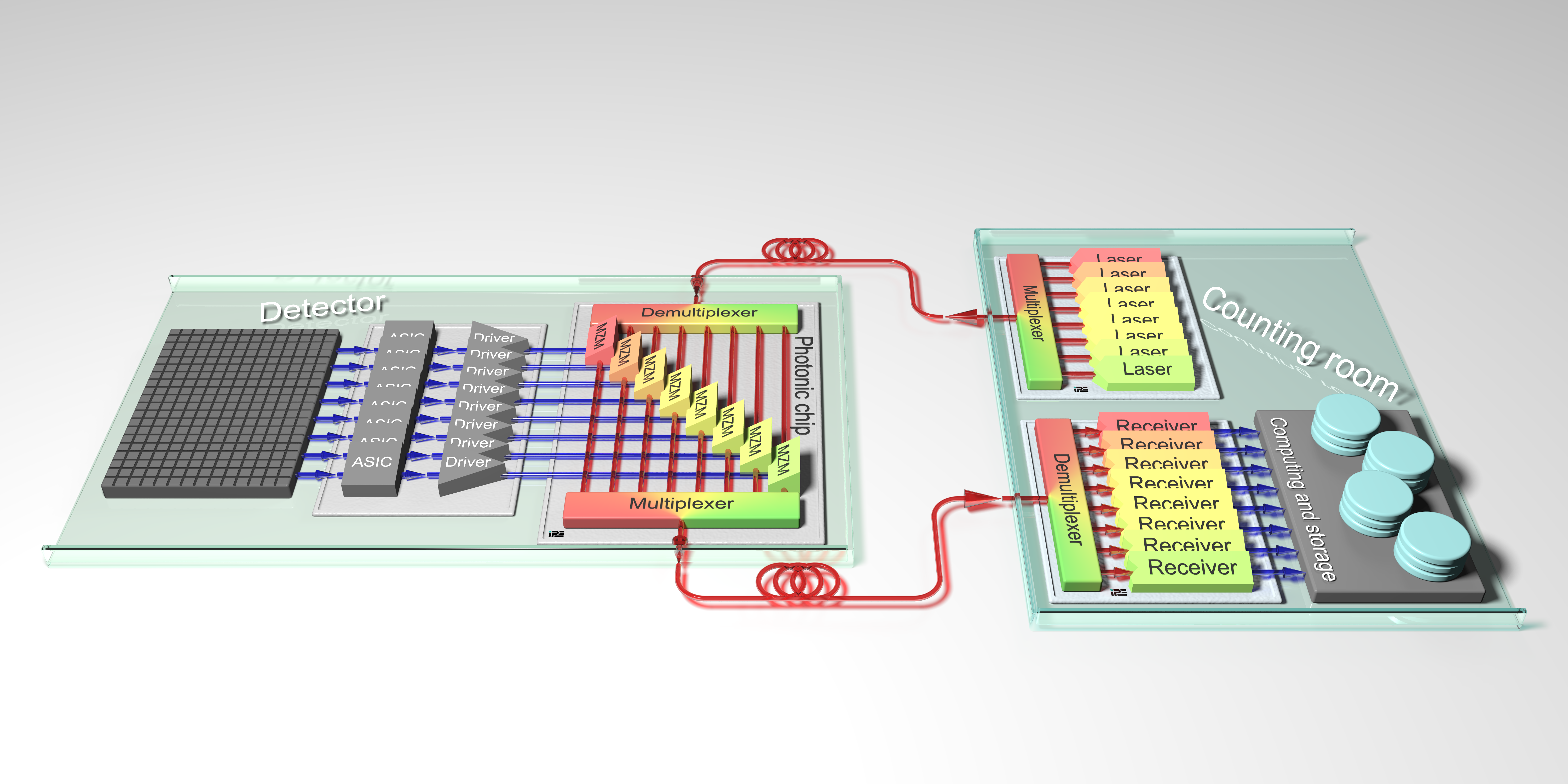
In our system, the lasers are located outside the detector. Therefore they are not affected by particle bombardment or radiation exposure and standard components from telecommunication technology can be used. In addition, the space requirements and energy consumption inside the detector volume can be significantly reduced. The wavelength division multiplexing (WDM) technique reduces the required number of optical fibers considerably. Many individual lasers generate optical carriers of different wavelengths. These are combined, transmitted through a single glass fiber, and directed to the transmitter chip in the detector. An optical demultiplexer is located on the chip, which splits the light by wavelength and feeds it to many electro-optical modulators. Each modulator encodes an electrical data signal onto the optical carrier. All modulated signals are recombined by an optical multiplexer and fed back into the counting room via another optical fiber. In the counting room is another demultiplexer located, which separates the optical signals by wavelength again and routes them to individual receivers for further processing.
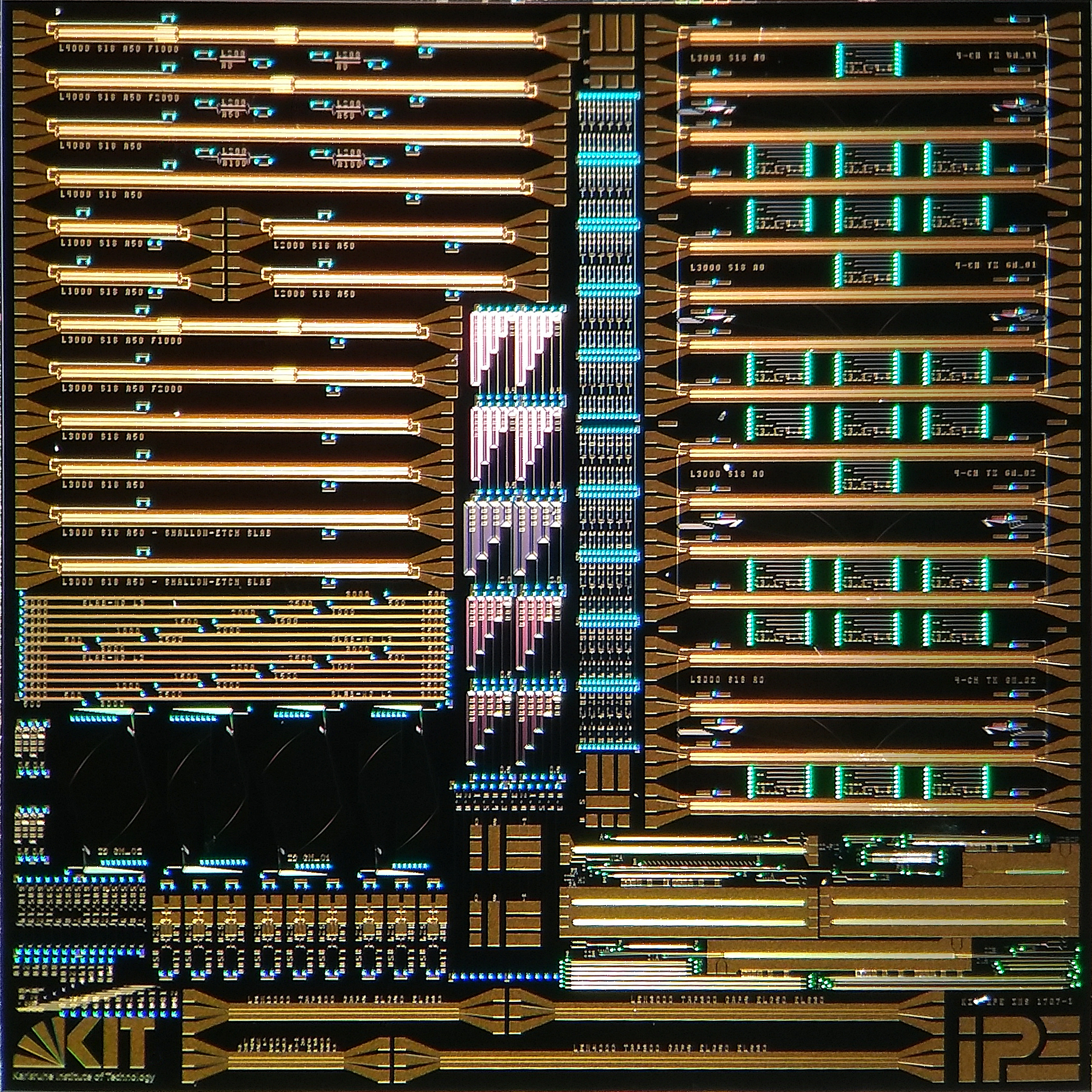
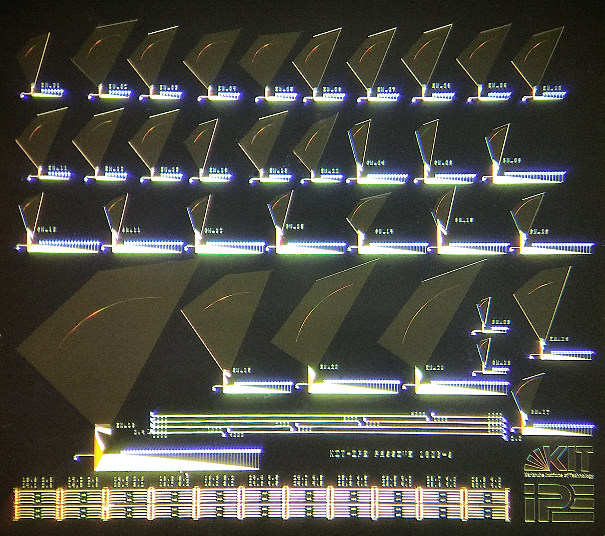
The use of electro-optical modulators in Mach-Zehnder design offers the advantage of energy-saving components that can deliver a very high transmission bandwidth of over 40 Gbit/s. By using higher modulation formats than on-off keying, such as phase shift keying (PSK) and multilevel amplitude modulation (xASK), even significantly higher bandwidths are possible. Parallelisation via WDM then allows transmission bandwidths in the range of several terabits/s per fibre to be achieved. We have already implemented (de-)multiplexers with up to 45 channels and even more channels appear feasible.
By using silicon as the photonic platform, monolithic integration of the driver electronics is also possible, which can significantly simplify the packaging and interconnection technology, especially with many wavelength channels. By following certain design rules, both the driver electronics and the silicon photonic components can be made radiation resistant.
Such an approach is completely new in the field of complex detector systems and could revolutionize the methods of data acquisition and transmission. Compared to currently used transmission systems, this technology makes it possible to reduce the energy requirements in the detector and increase the data throughput per fiber by several orders of magnitude. As a result, considerably fewer data lines and possibly also power supply cables and cooling pipes are required. By saving material and space, the tracking accuracy in particle physics experiments can be increased.
We design and simulate the silicon photonic devices. From these we develop integrated photonic chips, for which layouts are created for production by external chip manufacturers. The finished chips are then characterized in our laboratories and integrated into the entire system.
For the operation of the modulators, we develop driver circuits which on the one hand amplify the data signals with high bandwidths to the required voltage levels and on the other hand enable operating point adjustments of the individual modulators. Additional monitoring and parameterization functions are integrated for the permanent and reliable operation of the entire transmission system.
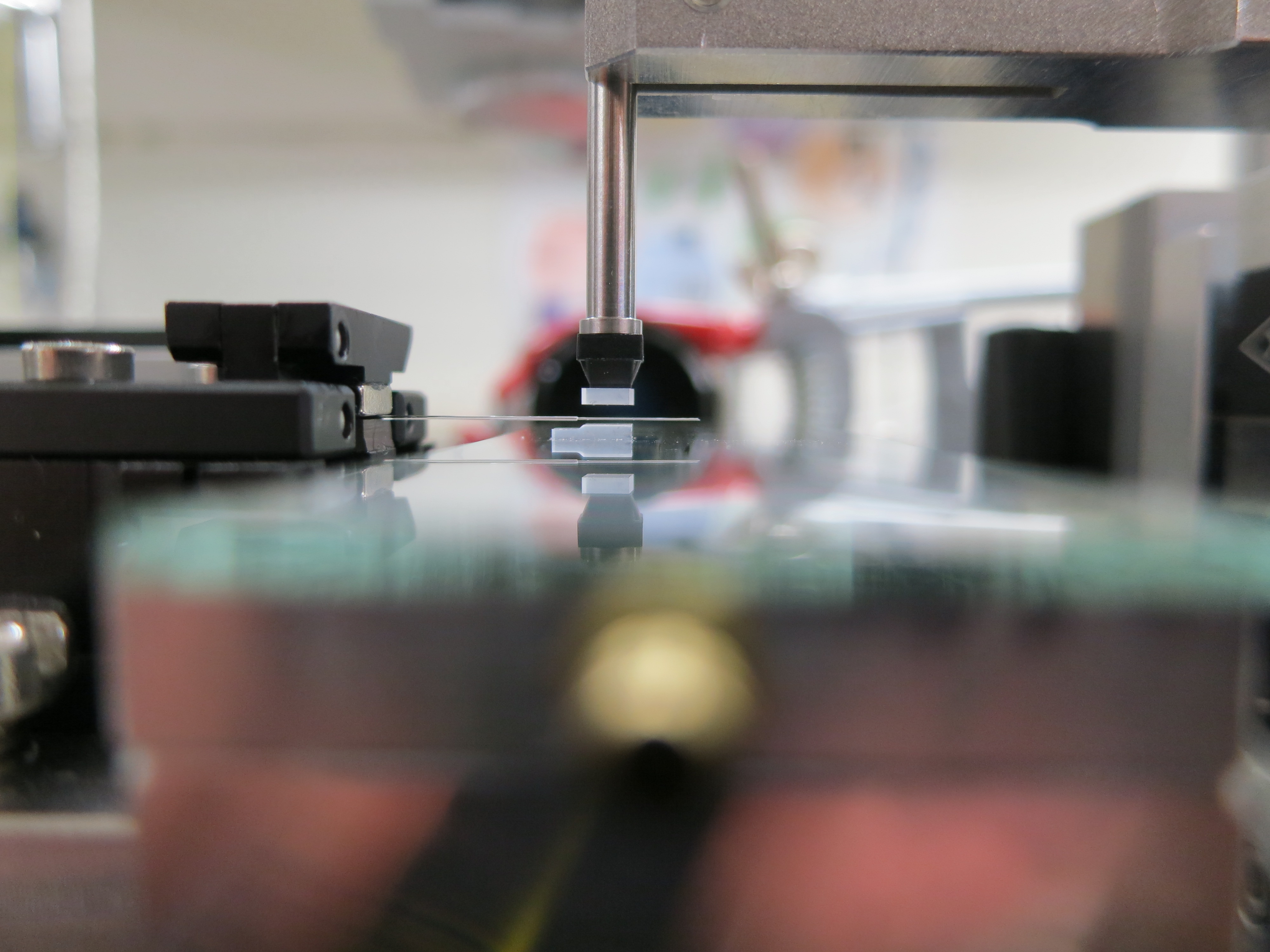
For system integration, the coupling of optical fibers to photonic chips (fiber-chip coupling) with tolerances in the sub-micrometer range represents a particular challenge. On the one hand, the design is subject to the limited space available in the detector. On the other hand, the stability of the coupling must be guaranteed even under demanding environmental conditions such as low temperatures. We have already developed a process for a compact design. However, this is only suitable for laboratory quantities so far. Therefore, the development is far from being finished here as well.
In cooperation with CERN, INFN Pisa, and the University of Bristol we develop modulators based on optical ring resonators for the transmission system. Ring modulators filter out exactly the wavelength to be modulated and are very compact. Additional demultiplexers and multiplexers are not necessary here, so that much smaller transmitter chips could be realized with them. However, setting and maintaining their operating point is challenging and will also be subject of future developments.
For students
We are a small, interdisciplinary team at Campus North with well-equipped laboratories and workstations. System development offers challenges in the fields of semiconductor physics, photonics, electrical engineering, and packaging technology.
For all sub-areas we continuously offer bachelor and master theses to students from physics, electrical engineering, information technology and mechanical engineering. We would be pleased about active support for our team. If you are interested, have a look at the advertised theses or simply contact Marc Schneider.
Publications
Schneider, M.
2023, October 5. Topical Workshop on Electronics for Particle Physics (TWEPP 2023), Geremeas, Italy, October 1–6, 2023
Schneider, M.
2023, April 12. doi:10.5281/zenodo.7821562
Schneider, M.
2022, November 25. doi:https://doi.org/10.5281/zenodo.7361526
Zhang, Y.; Karnick, D.; Schneider, M.; Eisenblätter, L.; Kühner, T.; Weber, M.
2019. Topical Workshop on Electronics for Particle Physics (TWEPP2018) - Posters, Art.-Nr.: 057, Scuola Internazionale Superiore di Studi Avanzati (SISSA). doi:10.22323/1.343.0057
Schneider, M.
2022, September 20. Topical Workshop on Electronics for Particle Physics (TWEPP 2022), Bergen, Norway, September 19–23, 2022
Zhang, Y.; Schneider, M.; Eisenblätter, L.; Karnick, D.; Kühner, T.; Weber, M.
2020. Journal of Instrumentation, 15 (02), Art.-Nr.: P02022. doi:10.1088/1748-0221/15/02/P02022
Zhang, Y.; Schneider, M.; Karnick, D.; Eisenblätter, L.; Kühner, T.; Weber, M.
2019. Proceedings of Topical Workshop on Electronics for Particle Physics, TWEPP 2019, Santiago de Compostela, Spain, 2 - 6 September 2019, Code 160323. doi:10.22323/1.370.0050
Schneider, M.; Zhang, Y.; Karnick, D.; Eisenblätter, L.; Kühner, T.; Weber, M.
2019. Proceedings of Topical Workshop on Electronics for Particle Physics, TWEPP 2019, Santiago de Compostela, Spain, 2 - 6 September 2019, Code 160323, Scuola Internazionale Superiore di Studi Avanzati (SISSA). doi:10.22323/1.370.0053
Zhang, Y.; Schneider, M.; Karnick, D.; Eisenblätter, L.; Kühner, T.; Weber, M.
2020. Optical Interconnects XX, Ed.: H. Schröder, 112860Y, Society of Photo-optical Instrumentation Engineers (SPIE). doi:10.1117/12.2544694
Zhang, Y.; Schneider, M.; Karnick, D.; Eisenblätter, L.; Kühner, T.; Weber, M.
2020. Optical Interconnects XX . Ed.: H. Schröder, 112860P, Society of Photo-optical Instrumentation Engineers (SPIE). doi:10.1117/12.2544663
Karnick, D.
2020, March 9. Karlsruher Institut für Technologie (KIT). doi:10.5445/IR/1000105691
Zhang, Y.; Schneider, M.; Karnick, D.; Eisenblätter, L.; Kühner, T.; Weber, M.
2019. Journal of Instrumentation, 14 (08), P08021. doi:10.1088/1748-0221/14/08/P08021
Zhang, Y.; Schneider, M.; Karnick, D.; Eisenblätter, L.; Kühner, T.; Weber, M.
2019. M. J. Digonnet & S. Jiang (Eds.), Optical Components and Materials XVI. Ed.: S. Jiang, 18, Society of Photo-optical Instrumentation Engineers (SPIE). doi:10.1117/12.2507433
Karnick, D.; Eisenblätter, L.; Kühner, T.; Schneider, M.; Zhang, Y.; Weber, M.
2018. Topical Workshop on Electronics for Particle Physics (TWEPP 2018), Antwerp, Belgium, September 17–21, 2018
Schneider, M.; Karnick, D.; Eisenblätter, L.; Zhang, Y.; Hartmann, J.; Kühner, T.; Weber, M.
2018. sixth Common ATLAS CMS Electronics Workshop for LHC Upgrades (2018), CERN, Genf, April 24–26, 2018
Karnick, D.; Bauditsch, N.; Eisenblätter, L.; Kühner, T.; Schneider, M.; Weber, M.
2017. 67th IEEE Electronic Components and Technology Conference, ECTC 2017, Orlando, Florida, USA, 30th May - 2nd June 2017, 1627–1632, Institute of Electrical and Electronics Engineers (IEEE). doi:10.1109/ECTC.2017.245
Karnick, D.; Skwierawski, P.; Schneider, M.; Eisenblätter, L.; Weber, M.
2017. Journal of Instrumentation, 12 (03), C03078. doi:10.1088/1748-0221/12/03/C03078
Kaschel, M.; Letzkus, F.; Butschke, J.; Skwierawski, P.; Schneider, M.; Weber, M.
2016. Silicon Photonics and Photonic Integrated Circuits V, Bruxelles, B, April 3-7, 2016. Ed.: L. Vivien, 98911V, Society of Photo-optical Instrumentation Engineers (SPIE). doi:10.1117/12.2228817
Skwierawski, P.; Schneider, M.; Karnick, D.; Eisenblätter, L.; Weber, M.
2016. Journal of Instrumentation, 11 (1), C01045. doi:10.1088/1748-0221/11/01/C01045
Karnick, D.; Skwierawski, P.; Schneider, M.; Eisenblätter, L.; Weber, M.
2016. Semiconductor Detectors in Astronomy, Medicine, Particle Physics and Photon Science : 607.WE-Heraeus Seminar, Bad Honnef, February 15-17, 2016